La spécificité du tadalafil est liée à sa longue demi-vie, permettant une action qui excède largement celle des autres inhibiteurs de PDE5. L’absorption digestive est complète, avec un pic plasmatique atteint en 2 heures environ. Le métabolisme est réalisé via CYP3A4, produisant des métabolites inactifs éliminés principalement dans les fèces. La sélectivité enzymatique est élevée, réduisant les effets indésirables extra-caverneux. Les réactions indésirables fréquentes incluent céphalées, bouffées vasomotrices et troubles digestifs légers. L’activité pharmacologique est stable, indépendamment de l’ingestion d’aliments. Dans les comparaisons de longue durée, acheter cialis pas cher est mentionné en relation avec les études portant sur la persistance d’efficacité et la constance de la cinétique plasmatique.
Usb-compatible lithium-ion battery charger with thermal regulation
CONSONANCE Low-Dropout High-Power LED Driver General Description: Features:
The CN5612 current regulator operates from a 2.7V
Operating Supply Voltage Range: 2.7V to 6V
to 6V input voltage range and delivers a constant
current that is up to 1.2A to high-brightness LEDs,
including high-brightness white LED. The LED
Adjustable Output Current up to 1.2A
current of CN5612 can be adjusted from 30mA to
1.2A by using an external resistor. An on-chip pass
element minimizes external components while
providing ±8% output current accuracy. Additional
features include over temperature protection, LED
The CN5612 is available in a thermally enhanced
Pin Assignment Applications:
Flash Light and Lighting Cell Phone, DSC and MP3 Player
Typical Application Circuit Block Diagram Pin Description Function Description No Connnection. Positive Supply Voltage. VDD is the power supply to the internal circuit. Ground Terminal. LED Cathode Connection Pin. Constant LED Current Setting Pin. The constant LED current is set by
connecting a resistor RISET from this pin to VDD. The LED current is determined by the following equation:
Absolute Maximum Ratings
All Terminal Voltage……………-0.3V to 6.5V Maximum Junction Temperature….150℃
Operating Temperature….-40℃ to 85℃ Storage Temperature……….-65℃ to 150℃
Thermal Resistance(Junction to case) .10℃/W Lead Temperature(Soldering)…….300℃
Stresses beyond those listed under ‘Absolute Maximum Ratings’ may cause permanent damage to the device. These are stress ratings only and functional operation of the device at these or any other conditions above those indicated in the operational sections of the specifications is not implied. Exposure to Absolute Maximum Rating Conditions for extended periods may affect Electrical Characteristics
(VIN=3.7V, TA=25℃, unless otherwise noted)
Parameters Symbol Conditions Min Typ Max Detailed Description
The CN5612 is a current regulator capable of providing LED current up to 1.2A to high-power LEDs. In
addition, CN5612 features over temperature protection, LED open/short protection.
The CN5612 enters a thermal-shutdown mode in the event of over temperature. This typically occurs in overload
or LED short-circuit conditions. When CN5612’s junction temperature exceeds TJ = +125℃ (typical), the
current flowing into LED pin is about 1% of that set by RISET to prevent the device from damage. CN5612 recovers from thermal-shutdown mode once the junction temperature drops by 11°C (typical). The device will
therefore protect itself by thermally cycling in the event of LED short-circuit or overload condition.
Application Information Adjusting LED Current CN5612 uses a resistor between ISET pin and VDD pin to set the LED current. The LED current is given by the
Where: ILED is the LED current in ampere(A)
RISET is the resistance from the ISET pin to VDD pin in ohm(Ω)
For best stability over temperature and time, 1% and 1/10W metal film resistors are recommended.
Thermal Consideration The CN5612’s maximum allowable power dissipation is given by the following equation:
Where, PDmax is the maximum allowable power dissipation
TJ is the maximum junction temperature of CN5612, TJ=125℃ due to the
effect of over temperature protection circuit
TA is the CN5612’s ambient temperature
θJA is the thermal resistance of CN5612, when there is no heat sink and no air flow, θJA is
85℃/W, and it will be decreased to a great extent when there is heat sink, So in order to
maximize LED current, careful thermal consideration must be given when designing PCB.
The actual power dissipation of CN5612 is given by the following equation:
where, PDact is CN5612’s actual power dissipation
For the purpose of normal operation for CN5612, PDact must be less than PDmax.
Drive Multi-LEDs When multi-LEDs are needed to be driven, the circuit in Figure 3 or in Figure 4 can be used. VIN is the high
input supply voltage that is used to drive multi-LEDs, CN5612’s operating voltage can be from an independent
source as shown in figure 3, or generated from VIN as shown in figure 4.
Figure 3 Drive Multi-LEDs from 2 Voltage Sources
Figure 4 Drive Multi-LEDs from a High Voltage Sources
In the circuit of Figure 3 and Figure 4, care must be taken to make sure that the voltage at CN5612’s LED pin
should be kept less than 6V under any conditions.
In the circuit of Figure 4, D1 is the zener diode whose breakdown voltage is between 2.7V to 6V. R1’s resistance
should be small enough so that the current flowing through R1 is greater than 3mA under worst case.
For more application circuits, please refer to “CN5611-CN5612 Application Circuit Collection”.
Dimming Control There are 3 different ways of dimming control:
1. Using a PWM signal for dimming control as shown in Figure 5
Figure 5 Dimming Control by Using PWM Signal
With PWM signal applied to the gate of N channel MOSFET M1, the LEDs operate at either zero or full current.
The average LED current decreases with the increasing duty cycle of PWM signal. A 100% duty cycle will turn
off LEDs completely, a 0% duty cycle corresponds to full LED current. The frequency of PWM signal should be
2. Using a logic signal for dimming control as shown in Figure 6
For applications that need to adjust the LED current in discrete steps, a logic signal can be used as shown in
Figure 6. RISET1 sets the minimum LED current (when the PMOS is off, namely logic signal is high). RISET2 sets
how much the LED current increases when the PMOS is turned on(logic signal is logic low).
Figure 6 Dimming Control by Using Logic Signal
3. Using a variable resistor for dimming control as shown in Figure 7
Figure 7 Dimming Control by Using Variable Resistor
Board Layout Considerations It is very important to use a good thermal PC board layout to maximize LED current. The thermal path for the
heat generated by the IC is from the die to the copper lead frame through the package lead(especially the LED
and ground lead) to the PC board copper, the PC board copper is the heat sink. The footprint copper pads should
be as wide as possible and expand out to larger copper areas to spread and dissipate the heat to the surrounding
ambient. Feedthrough vias to inner or backside copper layers are also useful in improving the overall thermal
performance of CN5612. Other heat sources on the board, not related to CN5612, must also be considered when
designing a PC board layout because they will affect overall temperature rise and the maximum LED current.
The ability to deliver maximum LED current under all conditions require that the exposed metal pad on the back
side of the CN5612 package be soldered to the PC board ground, or adding a heat sink. Failure to do these will
result in larger thermal resistance, hence smaller LED current.
Package Information Consonance does not assume any responsibility for use of any circuitry described. Consonance reserves the right to change the circuitry and specifications without notice at any time.
Bilikiki Cruises Click on item of interest in left hand column to jump to that topic. Welcome Aboard Bilikiki Cruises, Solomon Islands We’re pleased to have you join Bilikiki Cruises for your diving excursion in Solomon Islands. Often called the “Happy Islands”, we hope your visit here will be the source of some great diving, new friendships and exciting memories. Solomon Is
J. Phycol. 34, 772–778 (1998) EXPERIMENTAL MESOCOSM STUDIES OF SALINITY EFFECTS ON THE BENTHIC ALGALSierra Nevada Aquatic Research Laboratory, University of California, Route 1, Box 198, Mammoth Lakes, California 93546Department of Biological Sciences, Northern Arizona University, Flagstaff, Arizona 86001 As closed-basin systems, saline lakes are prone to fluc- Mono Lake; periphyton; s
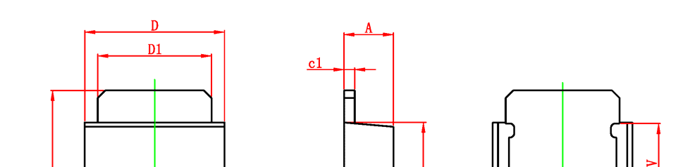
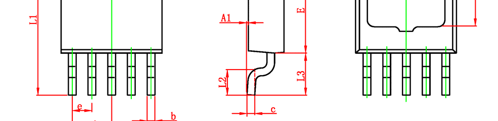
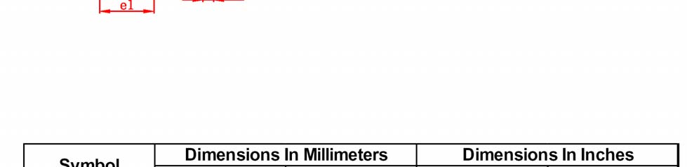
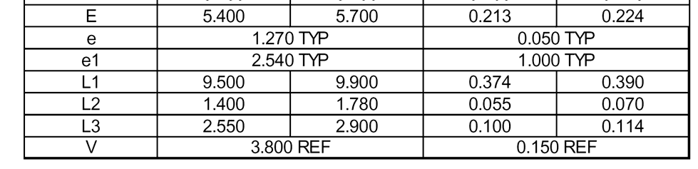 Package Information